DYMET
Technology & Equipment
DYMETTechnology & Equipment |
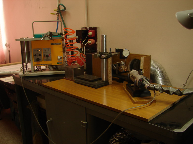
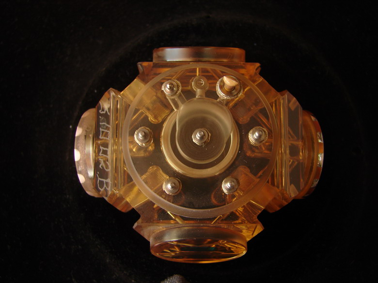
Special optical-electronic devices are produced at the laboratory.
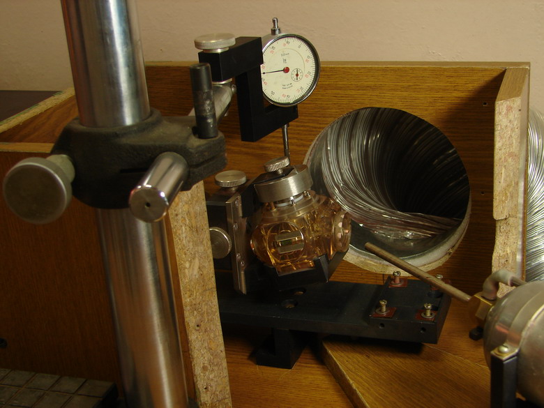
Metalization of some areas at the sitall surface may be performed just at the assembled device.
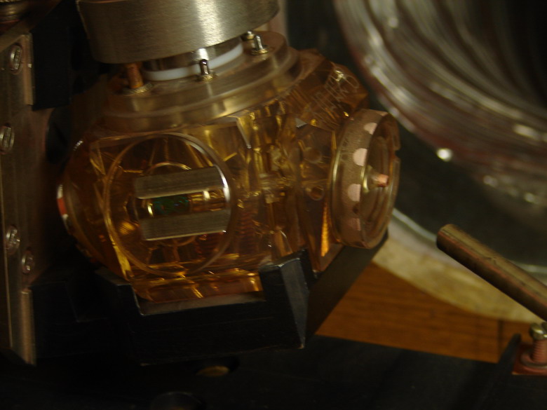
Coating is sprayed to some device areas for soldering.
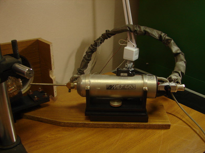
Nozzle position is varied because of specific shape of device.
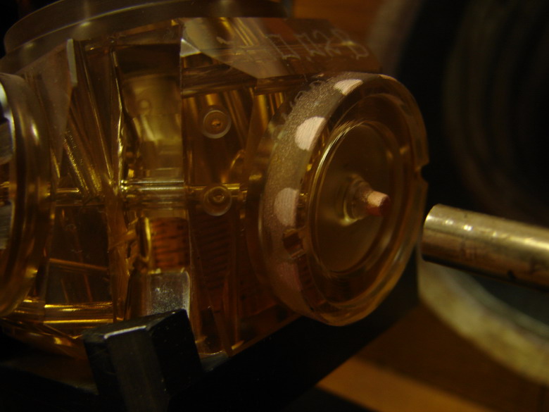
To limit metalization area special metal masks are used.
Sprayed areas are soldered after metalization.
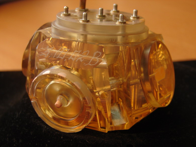
Bond strength of coating at contact areas is about 40 MPa.